

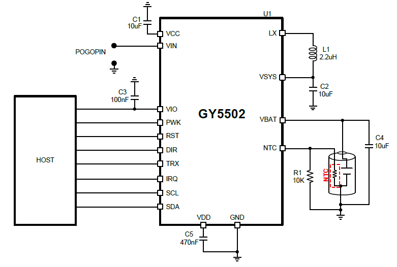
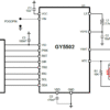
GY5502 is a highly integrated power management IC designed specifically for wearables and TWS earbuds. It offers a compact and efficient solution combining charging control, power path management, and power line communication into a single chip. The device supports NVDC architecture, configurable charging current and voltage, bidirectional single-line communication, battery gauge, 12-bit SAR ADC, and an I²C interface.
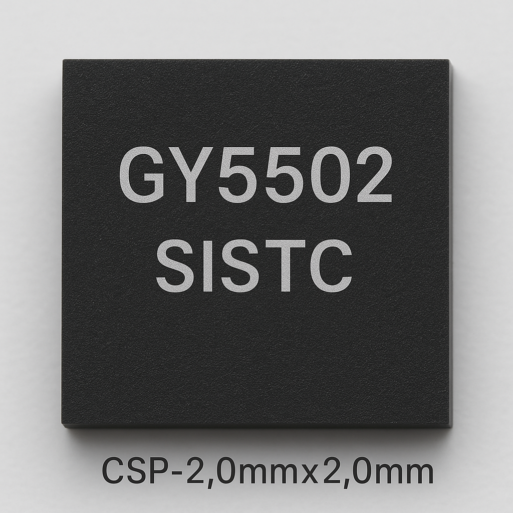
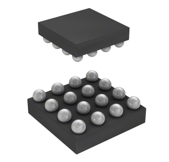
Its compact 2.0mm x 2.0mm CSP package makes it ideal for space-constrained applications.
Key Features
VBAT standby current: 3μA
Ship-mode standby current: 400nA
Input voltage withstand: VIN up to 16V
Input over-voltage protection (OVP): 6.0V / 6.8V
Constant charging current: 2mA to 500mA, register configurable
Charging voltage (VFLOAT):
4.00V–4.10V (step: 25mV), accuracy ±0.5%
4.10V–4.50V (step: 12.5mV), accuracy ±0.5%
Termination current (ITC/ITERM): 1mA to 40mA, configurable
DCDC charging supported, efficiency up to 93%
Bidirectional communication up to 3Mbps
Auto/manual direction switching
Supports voltage mode Rx/Tx and current mode Tx
Earbuds case-in/out detection integrated
Watchdog timer: 40s / 80s / 160s
I²C interface: up to 400kbps
12-bit SAR ADC: VIN, VBAT, NTC, ICC, IVIN monitoring
Integrated battery gauge (±5% accuracy)
CSP package: 2.0mm × 2.0mm
Applications
True Wireless Stereo (TWS) earbuds
Smartwatches and fitness trackers
IoT wearable devices
Smart rings and compact healthcare devices